
Nuevo avance en la tecnología IBC: desarrollo de células solares SABC de contacto posterior autoalineadas basadas en deposición física de vapor (PVD)
Las células solares de contacto posterior interdigitado (IBC) ofrecen un alto potencial de eficiencia gracias a su diseño sin electrodo frontal y a sus características de contacto pasivado de doble cara. Sin embargo, el proceso tradicional de fabricación de células IBC es complejo e implica múltiples etapas de dopaje y modelado de electrodos, lo que incrementa el coste y la dificultad de fabricación. La tecnología SABC propuesta en este artículo simplifica significativamente el flujo del proceso mediante la deposición de una capa de polisilicio tipo n mediante PVD y su combinación con separación autoalineada.
Las células solares SABC son una tecnología avanzada de contacto posterior (BC). Su característica principal es la separación de los electrodos positivo y negativo en la parte posterior de la célula mediante tecnología de autoalineación, lo que mejora la eficiencia y el rendimiento de la célula.
Método de fabricación de células solares de contacto posterior autoalineado (SABC)
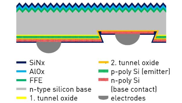
Estructura de celda solar SABC (contacto posterior autoalineado)
Superficie frontal:
●Capa de pasivación AlOx/SiNx: se utiliza para reducir la recombinación de la superficie y mejorar la eficiencia de captura de luz.
●Sustrato de silicio tipo n: el material principal del solar celúla.
Superficie posterior:
●TLa primera capa de óxido de tunelización: ubicada entre el polisilicio tipo p (p-poli Si) y el silicio SSustrato, utilizado para la pasivación y para promover el transporte selectivo de portadores.
●Capa de polisilicio tipo p (p-poli Si): actúa como emisor y forma una unión de efecto túnel con la capa de polisilicio tipo n.
●Capa de polisilicio tipo n (n-poli Si): Cubre el emisor de polisilicio tipo p y el sustrato de silicio expuesto (contacto base). Mediante deposición direccional por PVD, se desconecta automáticamente en la zanja debido al efecto de sombra para lograr una separación autoalineada.
●La segunda capa de óxido de tunelización: ubicada entre el polisilicio tipo p y el tipo n, optimiza el transporte de portadores.
●Electrodo metálico: capa de metalización impresa en un solo paso que cubre todas las áreas de polisilicio tipo n (contactos de emisor y base).
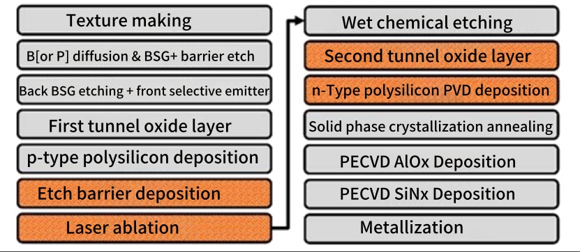
Proceso de fabricación de células solares SABC
Ventajas estructurales: Mediante la tecnología de autoalineación, las células solares SABC logran una separación precisa de los electrodos positivos y negativos en la parte posterior, reduciendo los pasos de fabricación y mejorando la eficiencia de la celda.
Simplificación de procesos: En comparación con las células solares TOPCon tradicionales, las células solares SABC solo agregan dos herramientas adicionales (herramienta de ablación láser y herramienta de deposición PVD), lo que simplifica enormemente el proceso de fabricación.
Diseño completamente pasivado: Al utilizar tecnología de pasivación en la parte delantera y trasera, se reduce significativamente la recombinación de la superficie y se mejoran el voltaje de circuito abierto (Voc) y la corriente de cortocircuito (Isc) de la celda.
Metalización simple: Dado que la capa de polisilicio tipo n cubre toda la parte posterior, la misma suspensión se puede utilizar para la metalización de ambas polaridades, simplificando aún más los pasos de fabricación.
Rendimiento de los contactos pasivados de polisilicio tipo n
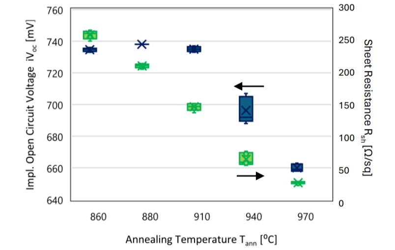
Rendimiento de iVoc y resistencia laminar de contactos pasivados de polisilicio tipo n con PVD
Relación entre iVoc y la temperatura de recocido:
El iVoc más alto (738 mV) se alcanza a 880°Recocido C, pero la resistencia de la lámina es alta (208 Ω/cuadrado).
Baja temperatura (<860°C) conduce a una activación de dopaje insuficiente (aumento de Rsh) y a una temperatura elevada (>880°C) provoca la degradación de la capa de óxido de tunelización (disminución de iVoc).
Análisis SIMS: Concentración de fósforo (Cp=1×1021 cm−3) es similar a todas las temperaturas, pero la difusión de fósforo en el sustrato de silicio se agrava a altas temperaturas, lo que aumenta la recombinación Auger.
Es necesario equilibrar la calidad de pasivación (iVoc) y la conductividad (Rsh), lo que puede lograrse ajustando la tasa de deposición de PVD o la concentración de dopaje.
Pasivación y propiedades conductoras de pilas de polisilicio tipo p/tipo n
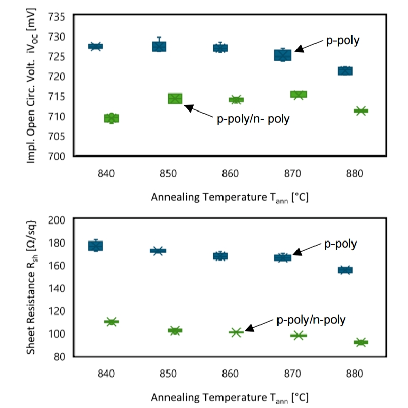
Rendimiento de la estructura apilada de poli-Si tipo p/poli-Si tipo n
Comparación de iVoc:
iVoc de capa única tipo p = 727 mV (870°C), mientras que la pila p/n iVoc = 715 mV, lo que indica que la capa de tipo n introduce una ligera pérdida de pasivación.
Resistencia de la lámina:
Rsh = 97 Ω/sq para la estructura apilada, significativamente menor que la de una sola capa de tipo n (208 Ω/sq), atribuido a la conducción paralela de las capas tipo n y tipo p. El valor calculado concuerda con el valor medido, lo que confirma las características de baja resistencia de la unión túnel.
La pérdida de pasivación puede ser causada por defectos en la interfaz entre el polisilicio tipo n y la capa tipo p, que deben mejorarse optimizando la capa de óxido de la interfaz.
Estructura de zanja y separación autoalineada de polisilicio tipo n
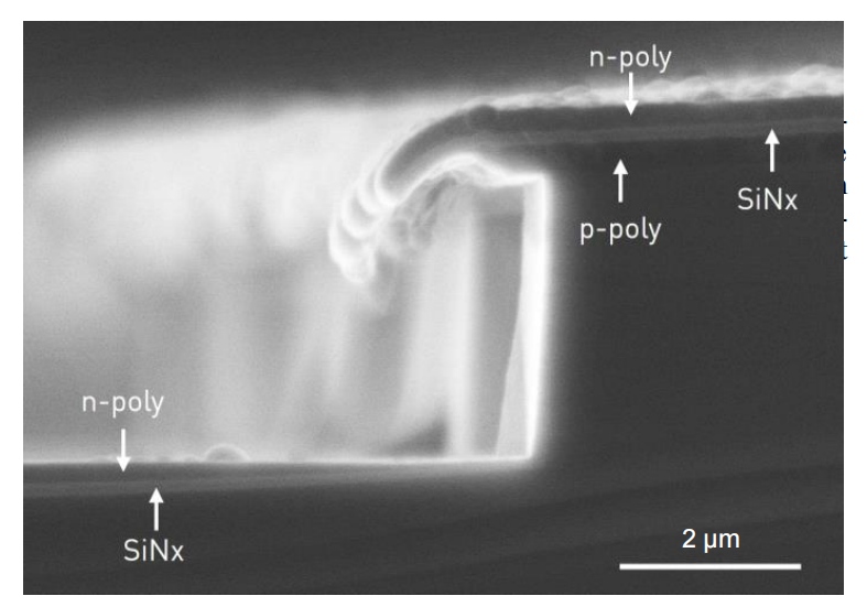
Imagen SEM de la sección transversal de la zanja
voladizo de polisilicio tipo p:
El espesor es de aproximadamente 300 nm y permanece en la parte superior de la zanja debido a las diferencias en la velocidad de grabado (p-poli Si < c-Si). Sobresale aproximadamente 1–1.5 μm horizontalmente, formando una estructura de "techo", que proporciona protección contra la sombra para una separación autoalineada.
Capa de polisilicio tipo n (n-poli Si):
Área continua: Espesor uniforme en el fondo de la zanja y el área plana (120–130 nm).
Área de separación: Se adelgaza gradualmente hasta desaparecer por debajo del saliente, lo que confirma las características de deposición direccional del PVD.
Capa auxiliar de SiNx:
Se utiliza solo para comparación de imágenes SEM, el espesor es de aproximadamente 100 nm, lo que distingue claramente el polisilicio del sustrato c-Si.
Profundidad de grabado:
La profundidad de la zanja es de aproximadamente 1,6 μm, lo que indica que la tasa de eliminación del grabado isotrópico del c-Si es significativamente mayor que la del polisilicio de tipo p.
La separación autoalineada se logra mediante deposición direccional por PVD y grabado de los voladizos. Esta estructura evita los complejos pasos de modelado del IBC tradicional y permite un espaciado ultraestrecho entre electrodos.
La separación autoalineada del polisilicio tipo n se logra mediante la tecnología de deposición física de vapor (PVD), lo que simplifica con éxito el proceso de fabricación de las celdas solares tradicionales de contacto posterior interdigitado (IBC). Los resultados experimentales demuestran que esta tecnología no solo logra un excelente rendimiento de pasivación (iVoc = 738 mV) y una baja resistencia laminar (Rsh = 97 Ω/sq), sino que también evitan procesos complejos de fotolitografía a través de la separación autoalineada de estructuras de trinchera, lo que proporciona un camino técnico factible para celdas IBC eficientes y de bajo costo.


 español
 English
 한국의
한국의


 Soporta red IPv6